UNDERSTAND WHAT THE HERO UNDERSTOOD
Why Noyce?
Noyce made complete circuits practical to mass-produce on silicon.
Noyce saw how to connect electronic components on a single piece of silicon. His approach helped turn complex circuits into patterns that could be manufactured in quantity—and opened a path toward the computing power we carry today.
Explore the idea Try it at homeTHE IDEA, AT YOUR PACE
Build a whole circuit together.
A computer built from separate parts.
Early transistor computers used circuit boards holding separate electronic parts. A transistor controls electric current; in a computer it can act as an electrically controlled on/off switch, with no moving lever. A circuit connects such parts so they work together—for example, to add two numbers. Picture assembling a board by hand: place a part’s metal leads through holes, then use a soldering iron to melt a small amount of solder at each joint. The cooled solder joins the lead to a conductive track on the board. Repeat for the other parts. More parts mean more leads to attach and joints to check.
What work could you save by forming several components and their connections together?
TRY IT AT HOME
Shrink a letter with light.
Cut a big letter. Use a magnifying glass to project a tiny copy onto paper. See how a lens can reproduce a pattern at a size your scissors could never cut.
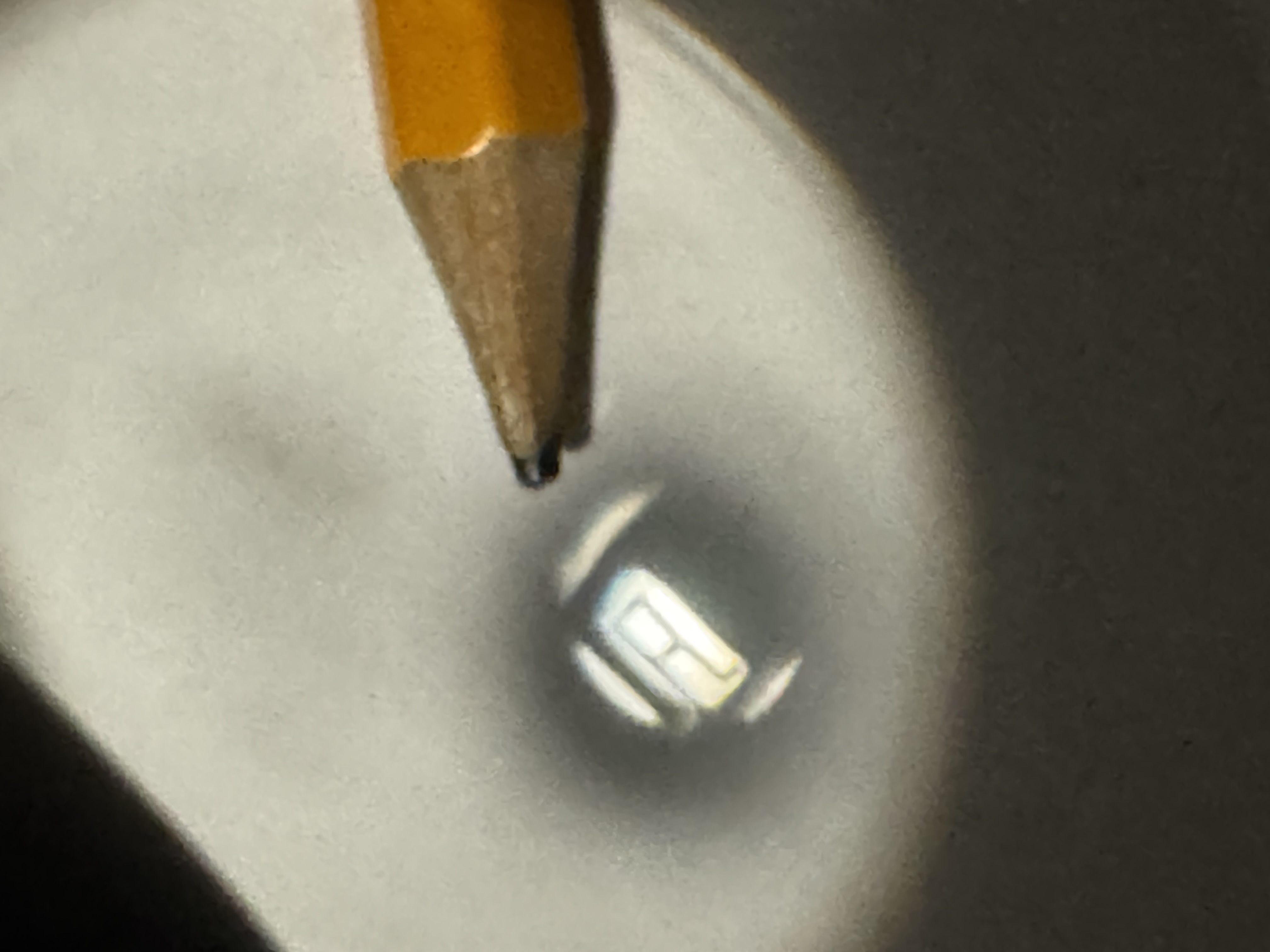
Gene tried this with his four-year-old son after they asked how chips are made. They cut his first initial into dark paper, then focused its image with a magnifying glass. The tiny “A” made the idea visible.
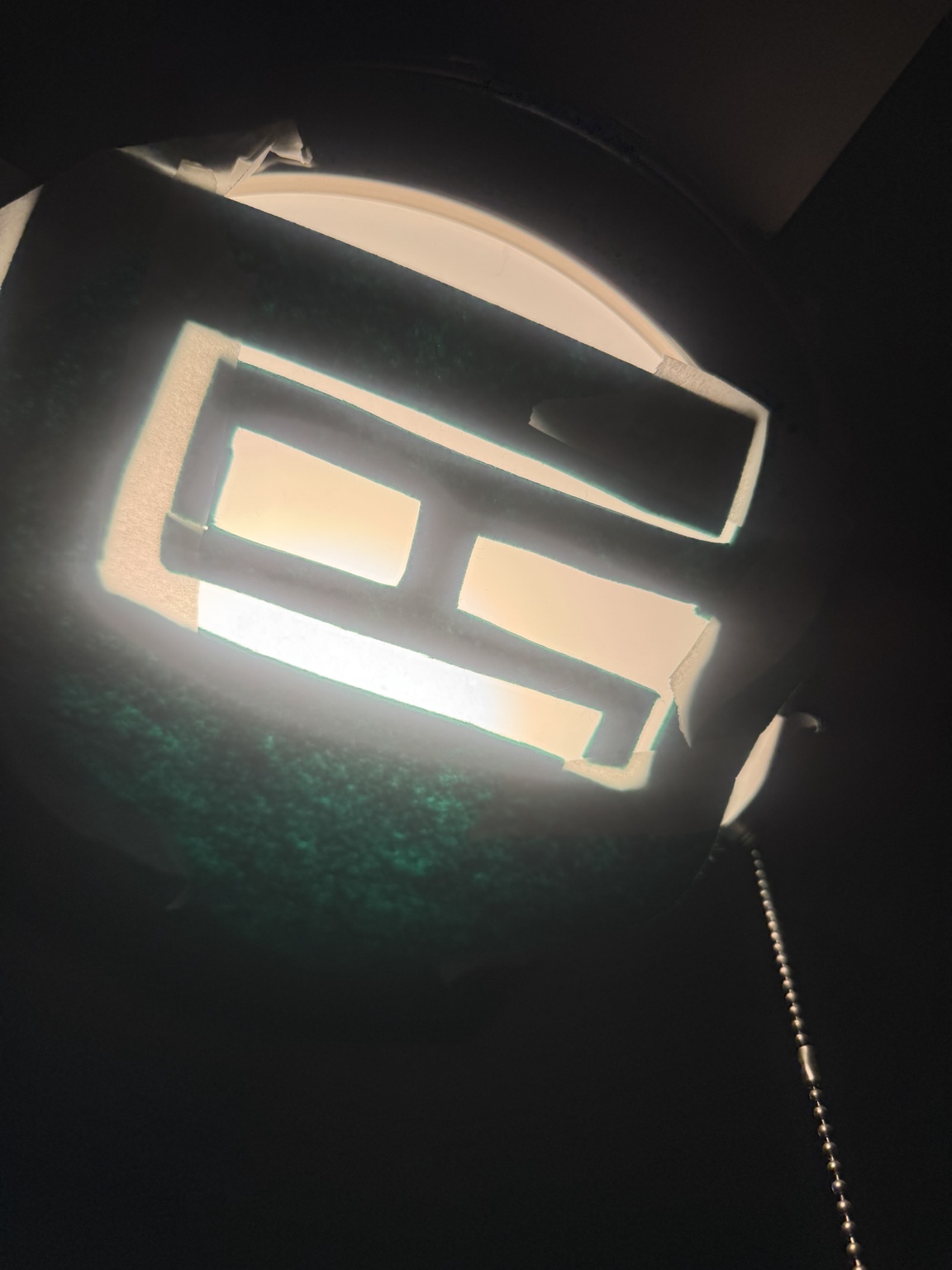
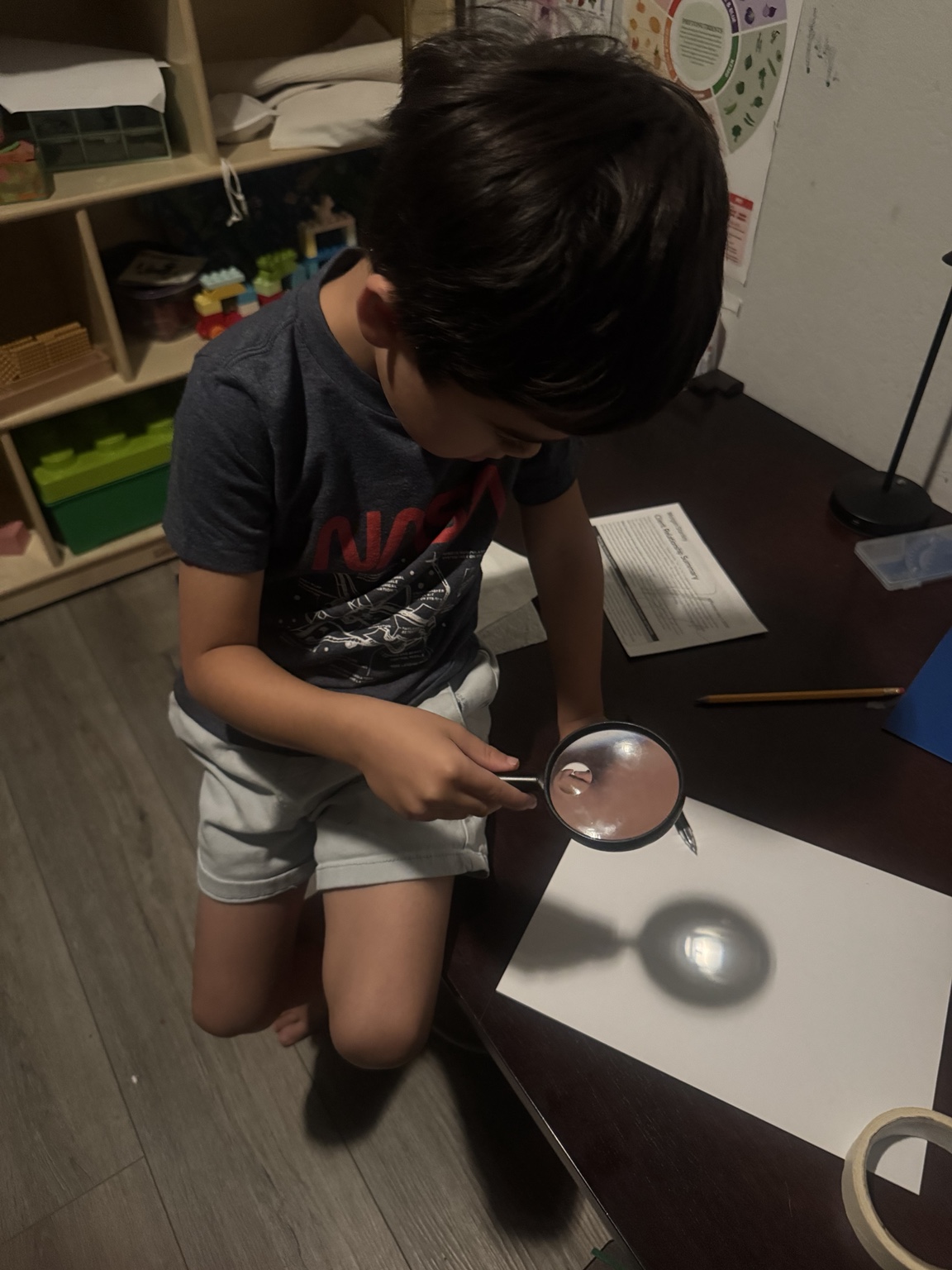
Make your own tiny initial.
Gather: thick dark paper, scissors, tape, a magnifying glass, white paper, a pencil, and an LED lamp.
Try this with an adult handling the cutting and lamp. Keep paper and tape clear of bulbs and vents. Use an indoor LED lamp; never use sunlight or a laser with the magnifying glass.
- Cut a letter. Have an adult cut a large A, T, or your own initial out of dark paper. Leave small paper bridges wherever an inside piece needs support.
- Light the stencil. Support the stencil upright in front of an LED lamp, with space between the paper and the lamp. Tape it to a separate cardboard support. Point the light through the cutout toward a clear tabletop.
- Line up the lens and paper. Place white paper on the tabletop in the path of the light. Hold the magnifying glass between the stencil and the paper, about a meter (3 feet) from the stencil and 4–12 inches from the paper. Keep the stencil and paper in place.
- Find the tiny letter. Move only the magnifying glass slowly toward or away from the paper until the letter is sharp. Different magnifying glasses focus at different distances. Set a pencil beside the image to compare their sizes.
Only a blur? Dim the other lights and keep the stencil and paper fixed. Move the magnifying glass slowly toward or away from the paper, keeping it lined up with the illuminated letter, until the image is sharp. The image may appear upside down.
Can you find the same crooked edge in the big cutout and the tiny letter? What happens when you slide the lens away?
Use light to carry a pattern.
The lens bends light from each point of the stencil to form an image on the paper. With the stencil far enough away and the paper at the right distance, that image is smaller. Lift the paper away and no mark remains on it: the pattern here is made of light.
In chipmaking, a light-sensitive coating called photoresist records a pattern. Development removes selected areas of that coating. For an oxide-opening step, chemical etching then removes the uncovered silicon dioxide, exposing the silicon beneath. Each step has a job: light defines the pattern; processing turns it into a physical structure.
Chip designers did hand-cut large patterns and photographically reduce them to make masks. Photolithography was already being developed for semiconductors in the 1950s. Noyce’s distinctive integrated circuit (IC) idea was metal connections over insulating oxide; optical patterning helped manufacture that structure. This home experiment explores image reduction. It leaves the chemical processing to the factory.
See historical hand-cut chip patterns · Computer History Museum ↗ACHIEVEMENT CAN STAND UP TO QUESTIONS
Ask the hard questions.
Yes. Kilby demonstrated a working integrated circuit at Texas Instruments in 1958. Noyce independently proposed a different approach in 1959: silicon devices connected by metal tracks over insulating oxide. Both are recognized as co-inventors, each for a distinct breakthrough.
Source: Noyce’s monolithic integrated circuit ↗THE EUDAIMONIA TEACHER
Ask Noyce’s world.
What part doesn’t make sense yet? Start there. Explore the science, the manufacturing, or why it matters.
An AI learning guide grounded in Noyce’s story. It does not speak as Noyce.
Checking teacher availability…
Follow the evidence
References from the Computer History Museum, the Smithsonian, and lithography manufacturer ASML. The teaching examples and “Why Noyce?” interpretation are Eudaimonia’s.